
RO4350B Process Dk vs Design Dk: Choosing and Verifying the Model
Updated October 13, 2026
A RO4350B stackup review often starts with two dielectric constants. The useful question is which value belongs in which decision, and how that decision will be verified on the finished circuit.
Use this guide when a schematic model, a fabricator’s impedance calculation and a laminate certificate appear to disagree. The workflow separates material identification, circuit modeling and production acceptance. Keeping those tasks separate makes a discrepancy easier to investigate and prevents a drawing from promising a property that nobody has agreed to measure.
Establish what the number describes
The Rogers RO4000 data sheet lists a process Dk of 3.48 ± 0.05 for the usual RO4350B construction, measured at 10 GHz and 23°C using clamped stripline. It separately lists design Dk as 3.66 using differential phase length over 8–40 GHz. A footnote identifies the 4 mil construction with process Dk 3.33 ± 0.05. Check the actual thickness and construction before copying a value into a procurement document.
These entries are different descriptions obtained under different conditions. A certificate that reports a process value does not automatically contradict a design model that uses another value. Conversely, a design model is not a replacement for verifying that the specified laminate was supplied. Record the source document, the relevant construction and the modeling purpose beside each number. An isolated spreadsheet cell labeled “Dk” does not carry enough information for a reliable handover.
The primary reference is the manufacturer’s RO4000 laminate data sheet. Use the material guide to assemble the rest of the construction specification.
Keep three quantities separate in the model
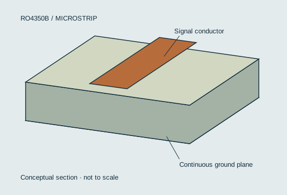
The dielectric input assigned to a substrate is one quantity. The effective permittivity of a transmission line is another. The impedance of the completed line is a third. They are related through geometry and electromagnetic boundary conditions, but they are not interchangeable labels for the same result. In particular, an exposed microstrip has fields in the dielectric and in the region above it. Its effective permittivity therefore needs to be calculated for that structure.
A solver may ask for a substrate material value and then calculate an effective result. Entering an already effective transmission-line value into the substrate field can apply the geometry adjustment twice. Before comparing two tools, inspect the meaning of their input fields. Also check whether the reported impedance is a single-ended characteristic impedance, a differential impedance or another quantity. A numerically plausible result can still answer the wrong question.
Write a short model card that another engineer can reproduce: structure type, signal layer, reference layer, dielectric height, conductor dimensions, mask coverage, dielectric input, frequency range and solver version. Include the assumed cross-section rather than only a screenshot of the final impedance. The cross-section reveals whether the tools are solving equivalent structures.
Work through a controlled sensitivity example
Consider an illustrative calculation in which the geometry factor stays fixed. In a simplified transmission-line model, impedance varies approximately with the inverse square root of effective permittivity. If the effective value changes from 2.80 to 2.90, the impedance ratio is the square root of 2.80 divided by 2.90, approximately 0.983. A nominal 50 ohm result would become about 49.1 ohms under this restricted assumption.
This calculation is a sensitivity example, not a material tolerance prediction. The two effective values were chosen to demonstrate the mathematics; they are not measured RO4350B production limits. It also assumes that conductor dimensions and all other boundary conditions remain fixed. A real change of laminate construction may change several parameters simultaneously, so the example cannot establish an acceptance range for a purchased board.
The same simplified model connects propagation delay to the square root of effective permittivity. A higher effective value means more delay for a fixed physical length. Consequently, a circuit can satisfy a fairly broad impedance requirement while still missing a tighter phase requirement. Decide whether impedance, phase, resonance position, insertion loss or several of these quantities control the application before selecting the verification method.
Compare calculations without changing several inputs at once
Start with the same cross-section in both tools. Match the units explicitly, including whether dielectric height excludes copper and whether the conductor thickness is the starting foil or the finished value. Use identical mask assumptions. If a model includes nearby ground copper, compare it with another model of the same coplanar structure rather than with an isolated microstrip equation.
Next vary one input while holding the others constant. Save the nominal case and two clearly labeled sensitivity cases. This exercise reveals which parameter changes the output most strongly for the particular geometry. It does not prove that the chosen variation represents the manufacturing distribution. Ask the fabricator for the appropriate dimensional information before turning a sensitivity sweep into a production tolerance analysis.
Do not tune the dielectric input simply until two tools produce the same answer. That approach can hide differences in conductor thickness treatment or reference-plane definition. First identify why the models differ. If an empirical correction is ultimately justified by measurements, label it as a calibrated model parameter and record the circuit, frequency range and process for which it was derived.
Plan a coupon that can answer the actual question
A useful coupon represents the production construction closely enough to investigate the design concern. Identify the signal and reference layers, geometry, mask condition, surface finish and expected measurement interface. If the objective is impedance acceptance, agree how the trace will be measured and which region of the result will be evaluated. If the objective is phase or loss correlation, define a suitable frequency-domain measurement and its reference planes.
Connector launches and fixtures contribute to a measured response. Decide how they will be characterized before ordering the coupon. A measurement across the complete fixture can be perfectly repeatable while still being unsuitable for extracting a substrate parameter. Keep the raw data, calibration information and any de-embedding method with the report so later reviewers can distinguish an instrument result from a processed estimate.
Use more than one structure when a single measurement cannot separate the unknowns. For example, a geometry measurement can constrain conductor width while an electrical measurement evaluates the resulting line. The broader principle is to avoid asking one number to identify several uncertain physical parameters simultaneously. A model that fits one coupon is useful evidence, but it still needs a defined range of applicability.
Translate the model into a fabrication drawing
The drawing should name the laminate grade and approved construction. It should separately define the controlled impedance targets, their tolerances and the relevant layers. Put the approved stackup and the trace structures under revision control. Avoid a note that simultaneously demands an exact simulated line width and permits unrestricted impedance compensation without explaining which requirement takes priority.
Request a documented proposal if the fabricator needs to change width, spacing or dielectric thickness. A change that improves a straight transmission line may also alter a coupled filter, a matching section or a connector launch. Mark those geometries clearly so manufacturing compensation is reviewed in the circuit context. Keep the approved change with the production files rather than leaving it only in an email exchange.
The procurement package should also state which records must accompany the lot. Material traceability, dimensional inspection and electrical results answer different questions. Agree the evidence needed for each requirement and who will accept a deviation. Our quality and acceptance planning guide provides a starting structure for this conversation.
Investigate a measured discrepancy in a practical order
First confirm identity: correct board revision, correct coupon, correct layer and correct file set. Then confirm the measurement setup and units. Review the physical construction before changing the material model. A misplaced reference plane, an unexpected mask layer or a different finished conductor thickness can invalidate an otherwise careful comparison.
After these checks, compare nominal and measured dimensions with the sensitivity cases. Look for a physically consistent explanation rather than the parameter that is easiest to edit. If the discrepancy remains, involve the fabricator and the material supplier with a concise package containing the construction, method, data and uncertainty. A request accompanied only by “the Dk is wrong” does not provide enough information to reproduce the observation.
When a correction is accepted, decide what must change: the simulation library, the drawing, the manufacturing process or the acceptance method. Record the reason and the affected products. Reusing a calibrated value in an unrelated stackup without reviewing the underlying conditions can recreate the original problem under a different name.
A release checklist for the design review
- Identify the exact material construction and the source of every dielectric input.
- Distinguish substrate input, effective permittivity and impedance in the model report.
- Match the modeled geometry to the proposed finished cross-section.
- Label illustrative sensitivity ranges separately from supplier tolerances.
- Define the electrical requirement that matters to circuit performance.
- Approve representative coupons, measurement interfaces and reporting rules.
- Preserve the stackup, compensation decisions and validation data with the revision.
For an initial geometry comparison, use the RO4350B microstrip estimator and read its assumptions. For a fabrication review, submit the stackup and controlled-impedance requirements with your files. Include the modeling value you used and the result you need verified; that gives the reviewer a clear technical question to resolve.