
RO4350B Core Thickness Selection: Geometry, Tolerances and Fabrication
Updated October 15, 2026
Choose RO4350B core thickness by reviewing the transmission line, component interface and manufacturing tolerances together. The mechanically convenient thickness is not automatically the electrically convenient one.
A core choice changes the space between a signal conductor and its reference plane. That changes the geometry required for a target impedance and can affect routing, transitions and sensitivity to dimensional variation. This guide provides a practical selection process for a new board or a revision that needs a different core. The numerical examples illustrate geometry relationships; they are not production stackup recommendations.
Define which thickness the drawing means
Before comparing alternatives, distinguish dielectric thickness from the complete copper-clad core thickness and the finished board thickness. A nominal dielectric dimension does not include every coating, conductor or bonding layer in a completed assembly. Different documents may use “board thickness” loosely, so specify the physical boundaries of each dimension in the stackup.
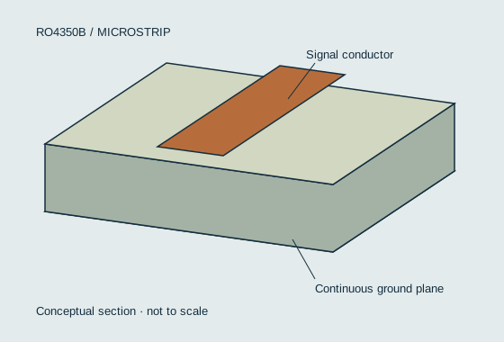
For an outer microstrip, the relevant dielectric height is the separation between the signal conductor and its reference plane. For a multilayer structure, the selected core may not be the only dielectric contributing to the fields. Identify the actual signal and reference layers rather than assuming that a catalog core label supplies every dimension needed by the electromagnetic model.
Prepare a cross-section with layer names, dielectric materials, nominal dimensions, copper and any mask. Give each thickness a unique label. When a supplier returns a proposed stackup, compare those labeled dimensions directly. This simple discipline prevents an overall-thickness agreement from being mistaken for agreement on the RF dielectric spacing.
Start from the circuit and mechanical interfaces
List the components that constrain the geometry. A connector launch may depend on a particular board edge and layer arrangement. A packaged device may present a narrow pad that needs a transition into the transmission line. A housing can constrain the overall board thickness while leaving some freedom in the RF core. Establish which restrictions are fixed and which can be negotiated before choosing a material thickness.
Next identify the electrically sensitive structures. Long feed lines, coupled sections, distributed matching networks and resonators do not all respond to a thickness change in the same way. A straight line can often be retuned by changing width, but that does not prove that nearby coupled structures or launches will preserve their response. Mark those structures for a separate review.
Connect the initial decision to the application requirements. A compact filter, a power amplifier output network and a measurement fixture can reasonably prioritize different constraints. The objective is to select a construction that supports the complete design, rather than to identify a universal best core for the material family.
Understand the width-to-height relationship
In a simplified zero-thickness microstrip model with a fixed dielectric input, characteristic impedance depends strongly on the ratio of conductor width to dielectric height. Scaling width and height together preserves that ratio. This provides a useful first comparison of candidate geometries, but it does not preserve every property of the physical circuit.
For an illustrative example, take a width of 1.10 mm over a dielectric height of 0.508 mm. The width-to-height ratio is approximately 2.17. Reducing the height to 0.254 mm and the width to 0.55 mm keeps the same ratio. An idealized model can therefore predict the same nominal impedance for both structures when its other assumptions remain unchanged.
That result does not mean the two constructions are interchangeable. Real copper thickness does not necessarily scale, nor do connector pads, surface roughness, mask thickness or fabrication tolerances. Conductor loss and discontinuity behavior also require separate consideration. Use the ratio argument to create a starting geometry, then review the actual finished structure with a suitable solver and the fabricator.
Compare sensitivity as well as nominal impedance
Suppose two candidate trace widths are 0.55 mm and 1.10 mm. An illustrative absolute width change of 0.025 mm represents about 4.5 percent of the narrower trace and about 2.3 percent of the wider trace. These percentages describe geometry only; they are not impedance percentages and the width variation is not a claimed supplier capability.
The example shows why a nominally correct impedance is insufficient for selection. Evaluate the response to plausible finished dimensions for each construction. Obtain the relevant process information from the fabricator instead of assuming that every candidate has the same absolute or relative tolerance. A design with more nominal margin can still be difficult to reproduce if a critical dimension is poorly constrained.
Build a small sensitivity table covering dielectric spacing, conductor width and conductor thickness. Identify which variations are independent and which are coupled by the process. Keep a conservative screening calculation separate from a statistical yield prediction. The latter requires information about distributions and correlations that a simple minimum-and-maximum table does not supply.
Review the copper construction when the core changes
Specify the foil construction and finished conductor requirement alongside the dielectric. A core substitution accompanied by a foil substitution changes more than thickness. Likewise, the starting foil designation does not alone define the final outer-layer copper after processing. Ask the fabricator to identify the dimensions used in its impedance calculation and the stage of manufacture they represent.
The manufacturer provides separate information for standard and LoPro constructions. Consult the relevant RO4000 LoPro processing guidance when that construction is proposed. A process recommendation for one construction should not be silently treated as approval for another.
Keep any thickness-specific material notes attached to the candidate stackup. The material specification should identify the exact grade and construction, not just the family name. If the modeled dielectric input came from a previous design, review its applicability before carrying it into a substantially different core or copper configuration.
Check transitions and return paths
A thinner dielectric can produce a narrower impedance-controlled trace, which changes the transition from a component pad or connector pin. Inspect the length and shape of that transition. Do not retain an old launch solely because the new straight-line section calculates to the same impedance. The fields near the launch depend on the complete local geometry.
For layer changes, include the via structure and its return path in the review. Overall board thickness, unused via length and plane arrangement may change independently of the outer RF core. A core change intended to simplify routing can therefore create a different transition problem elsewhere. Mark the reference plane used by each line segment and inspect how the return current moves between planes.
Nearby copper and mechanical metal also belong in the boundary conditions when they significantly affect the structure. A soldered shield, housing wall or mounting arrangement can make an isolated-line approximation incomplete. The right modeling detail depends on the circuit, but the decision to omit a feature should be deliberate and documented.
Ask for manufacturing feedback before layout is frozen
Send the candidate stackups, critical geometry and quantities to the fabricator early. Request confirmation of material availability, proposed finished dimensions and any process limitations relevant to the design. Avoid choosing a construction exclusively from a generic online list and discovering after layout that the proposed build requires a substitution.
Ask how the supplier intends to achieve the impedance target. The response should distinguish nominal design dimensions from manufacturing compensation. Define which changes can be made within an approved range and which need engineering approval. Coupled structures and component interfaces often deserve explicit protection from routine changes intended for uniform lines.
Discuss inspection evidence at the same time. If dielectric thickness is central to a model correlation, identify how representative dimensions will be measured and reported. If impedance is the purchase acceptance criterion, define the coupon and method. See the fabrication planning guide for the rest of the release package.
Use a decision record for the final choice
Record the alternatives that were actually evaluated, the constraints that eliminated them and the evidence supporting the selected construction. This record need not be long. A table linking each requirement to a calculation, supplier response or planned test is often more useful than a lengthy narrative that does not identify the decision basis.
Separate verified information from open items. For example, a supplier may have confirmed material availability while the connector launch still needs simulation. Marking the stackup “approved” without identifying that open work can allow procurement to move ahead of the electrical review. Use explicit release conditions so the team knows when the package is ready for fabrication.
Preserve the selected stackup with the board revision and the associated model files. If purchasing later proposes another construction, compare it against that record. The earlier decision becomes a reusable engineering reference rather than a choice that must be reconstructed from scattered messages.
Validate the first manufactured construction
On the first build, compare the delivered stackup evidence and electrical results with the model assumptions. Investigate differences before using the design as a production baseline. A functional prototype is valuable, but successful operation alone may not show how much margin remains across manufacturing variation or the intended operating conditions.
Keep the measurement boundaries consistent with the design review. Document whether the response includes connectors and fixtures. If a discrepancy requires a geometry change, preserve the measured data that motivated it and the revised model. This creates a traceable path from the original thickness choice to the final validated construction.
For an initial comparison, use the microstrip estimator within its stated limitations. For a project review, upload the proposed stackup and fabrication files with the mechanical constraints, controlled-impedance targets and candidate core thicknesses. Those inputs allow a specific engineering discussion instead of a generic recommendation based only on the laminate name.